Non-thermal precision cutting · Optics & photonics
Cutting brittle optical materials without compromise
In optical manufacturing, a single chip or subsurface crack can render a component worthless — no matter how precise the geometry. With fused silica, sapphire, borosilicate glass, or quartz, the margin between a functional part and scrap is measured in microns, and most conventional cutting methods push you uncomfortably close to that line.
The problem
Brittle materials don’t forgive
Optical and photonics materials share a defining trait: they are brittle. Unlike metals, they can’t absorb energy through plastic deformation — mechanical or thermal stress propagates as cracks (lateral, radial, Hertzian) that extend unpredictably beneath the surface.
A 2025 review in the Journal of Materials Research and Technology documents the scope for fused silica: subsurface defects — microcracks, scratches, pitting — form during mechanical processing and “can seriously reduce the optical performance and durability” of the finished component (Cao et al., 2025). These defects are often invisible to surface inspection, buried tens of microns below the cut edge.
Wavefront
Degraded optical quality
Subsurface damage in a lens substrate or diffraction grating degrades wavefront quality.
Reliability
Failure initiation site
In an optical sensor housing, a subsurface crack becomes a failure initiation site.
Yield
Compromised die yield
In a semiconductor wafer, edge chipping compromises die yield.
Why conventional methods fall short
Heat and force both leave a mark
Laser cutting
Thermal damage & HAZ
Laser cutting is fast and programmable — but it is a thermal process. Cutting fused silica or borosilicate glass generates a heat-affected zone; research in Applied Physics A (2022) shows HAZ persists even with ultrafast burst-mode pulses, and Results in Physics (2022) confirms the intrinsic HAZ during pulsed laser processing “significantly affects the surface quality of fused silica optics.” For sapphire, laser cutting adds microcracking from thermal shock, recast layers, and residual stress that can cause delayed fracture.
Mechanical dicing
Edge chipping & geometry limits
Diamond-blade dicing is the workhorse of wafer singulation, but comes with well-documented edge chipping (30°, 60°, 90° and irregular modes) from radial and lateral crack systems propagating along crystallographic slip planes. Chipping worsens with brittleness and thinner wafers — and the method can only cut straight or circular geometries. For fused silica or quartz, these chipping levels are often unacceptable.
The common thread: both methods introduce energy the substrate cannot absorb gracefully. Heat creates thermal gradients; mechanical contact creates stress concentrations. Both leave subsurface damage that compromises the very optical properties the component was designed to deliver.
The solution · micro-abrasive waterjet
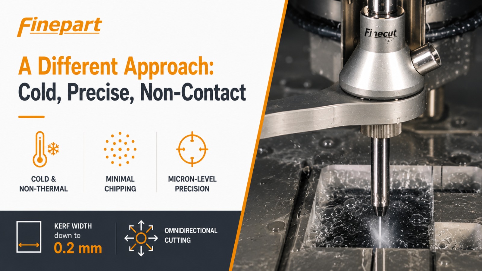
Cold, precise, non-contact
Micro-abrasive waterjet (MAW) cutting works on a fundamentally different principle. A fine stream of water at roughly 4,000 bar accelerates hard abrasive particles — typically garnet or alumina — through a nozzle as small as 0.2 mm. Material is removed by controlled particle erosion, not thermal ablation or mechanical shearing.
No heat-affected zone
Entirely non-thermal. No recast layer, no phase transformation, no residual thermal stress — optical and mechanical properties stay unchanged right up to the cut edge.
Minimal chipping
Material removal is gradual, distributed across thousands of micro-impacts rather than one concentrated force, so the fracture mechanics behind edge chipping are largely avoided.
Micron-level precision
A 0.2 mm kerf means minimal waste on expensive substrates, and because the jet acts at a single point it cuts omnidirectionally — enabling complex geometries.
Positional accuracy on the Finecut
State-of-the-art MAW systems such as the Finepart Finecut hold positional accuracy of ±1.5 µm and part tolerances down to ±10 µm, with surface roughness (Ra) down to ~0.8 µm — precision-optics territory.
Real-world validation
Wasatch Photonics
Wasatch Photonics — a leading manufacturer of volume phase holographic (VPH) transmission gratings, spectrometers, and OCT systems — adopted Finepart’s micro-abrasive waterjet technology for cutting optical components.
Edge quality
Higher precision
Cleaner, more precise cut edges on optical components.
Throughput
Increased capacity
More production output from the same process.
Design freedom
Complex geometries
Component shapes previously impractical or impossible with conventional methods.
For a company whose products depend on diffraction-grating-level precision, the choice of cutting technology is not incidental — it is imperative.
Where MAW fits
A precision tool in the photonics workflow
MAW is not a replacement for every step in optical fabrication. It is a precision cutting and shaping tool that fills a specific gap: near-net-shape optical blanks and components with no thermal damage and tight dimensional tolerances.
Substrates
Optical blanks
Fused silica, borosilicate glass, quartz.
Photonics
Components
Diffraction gratings, waveguide substrates, optical sensor housings.
Semiconductor
Wafer-level parts
Silicon and sapphire wafer singulation.
Ceramics
Precision components
Alumina housings, ceramic optical mounts.
Geometry
Complex 2D profiles
Shapes that would need multiple operations with conventional dicing.
Because the process preserves material properties at the cut edge, downstream finishing — lapping, polishing, coating — starts from a better baseline. In many cases secondary finishing can be reduced or eliminated entirely.
Materials cut on the Finecut micro-abrasive waterjet
Start with proof, not projections
Start with a proof of concept on your material
Managing chipping rates, rejecting parts for subsurface damage, or designing around the limits of thermal cutting? A proof-of-concept test cut is the most direct path to evaluation. Send a sample or a drawing; get cut parts back with measurable results — edge quality, dimensional accuracy, surface finish — on your actual production material.
No theoretical projections. Just data on your part.
References
- Cao, H., Peng, X., Shi, F., Tian, Y., Kong, L., Chen, M., & Hao, Q. (2025). Advances in subsurface defect detection techniques for fused silica optical components: A literature review. Journal of Materials Research and Technology, 35, 809–835. doi:10.1016/j.jmrt.2025.01.045
- Xie, X., Ou, D., Ma, D. et al. (2022). High-quality laser processing of fused silica with bursts of ultrafast pulses. Applied Physics A, 128, 1062. doi:10.1007/s00339-022-06218-0
- Heat accumulation effect during CO₂ laser processing of fused silica optics (2022). Results in Physics, 34, 105258. doi:10.1016/j.rinp.2022.105258
- Studies of chipping mechanisms for dicing silicon wafers (2006). International Journal of Advanced Manufacturing Technology, 29, 740–745. doi:10.1007/s00170-006-0800-3
- Cui, Y., Wang, C., Liu, X. et al. (2023). A review of subsurface damage detection methods for optical components. AIP Advances, 13(6), 060702. doi:10.1063/5.0151498
External research is cited to illustrate general material behaviour in optical and photonics manufacturing; it does not constitute endorsement of Finepart by the cited authors.
